The 7408 integrated circuit serves as a cornerstone in digital electronics. It contains four independent AND gates, each designed to perform logical operations with precision. Engineers and hobbyists rely on the ic 7408 for building circuits that require logical conjunctions. Its robust design and reliable performance make it essential for applications ranging from signal processing to control systems. Understanding the 7408 ic pin diagram and its truth table allows users to harness its full potential in digital projects.
Key Takeaways
-
The 7408 IC has four separate AND gates. It is important for digital circuits.
-
Knowing the pin diagram and pinout helps connect it correctly in systems.
-
The 7408 IC works well with different voltages. It can be used in simple circuits or big machines.
-
It switches quickly and uses little power, making it great for fast digital tasks.
-
Always check input voltages and pin connections to avoid damage and keep it working well.
Overview of the 7408 Integrated Circuit
The 7408 integrated circuit is a widely used digital logic IC that contains four independent AND gates. Its design ensures reliable performance in various electronic systems. Engineers and students often use the ic 7408 to implement logical operations in circuits due to its simplicity and efficiency. Understanding its features and applications provides insight into its versatility in digital electronics.
Key Features of the 7408 IC
The 7408 IC offers several features that make it a preferred choice for digital logic applications. It operates within a wide range of supply voltages and temperatures, ensuring compatibility with diverse systems. Below is a table summarizing its key parameters:
| Parameter | Value |
|---|---|
| Supply Voltage | Up to 7V |
| Input Voltage | Up to 5.5V |
| Operating Temperature | -55°C to 125°C |
| Storage Temperature | -65°C to 150°C |
| Supply Voltage Range | 4.75V to 5.25V |
| Input High Voltage (VIH) | At least 2V |
| Input Low Voltage (VIL) | No more than 0.8V |
| Output High Voltage (VOH) | At least 2.4V at 4mA |
| Output Low Voltage (VOL) | No more than 0.4V at 8mA |
| Power Dissipation | Uses up to 10mW per gate |
| Propagation Delay | 10 nanoseconds |
| Frequency Response | Up to several megahertz |
Tip: The low power dissipation and fast propagation delay make the 7408 IC ideal for high-speed digital circuits.
Common Applications of the 7408 IC
The 7408 integrated circuit plays a crucial role in various applications. Its ability to perform logical conjunctions makes it indispensable in digital systems. Below are some common uses of the ic 7408:
-
Basic Logic Circuits: The 7408 IC is often used to implement AND logic in simple circuits.
-
Microcontroller-Based Systems: It integrates seamlessly with microcontrollers to perform logical operations.
-
Signal Processing: Engineers use the 7408 IC to process signals in control systems and communication devices.
-
Arithmetic Operations: It assists in creating circuits for addition and multiplication using logical gates.
-
Industrial Automation: The IC contributes to automation systems by enabling logical decision-making processes.
The versatility of the 7408 IC ensures its presence in both educational projects and professional designs.
7408 IC Pin Diagram and Pinout
7408 IC Pin Diagram Overview
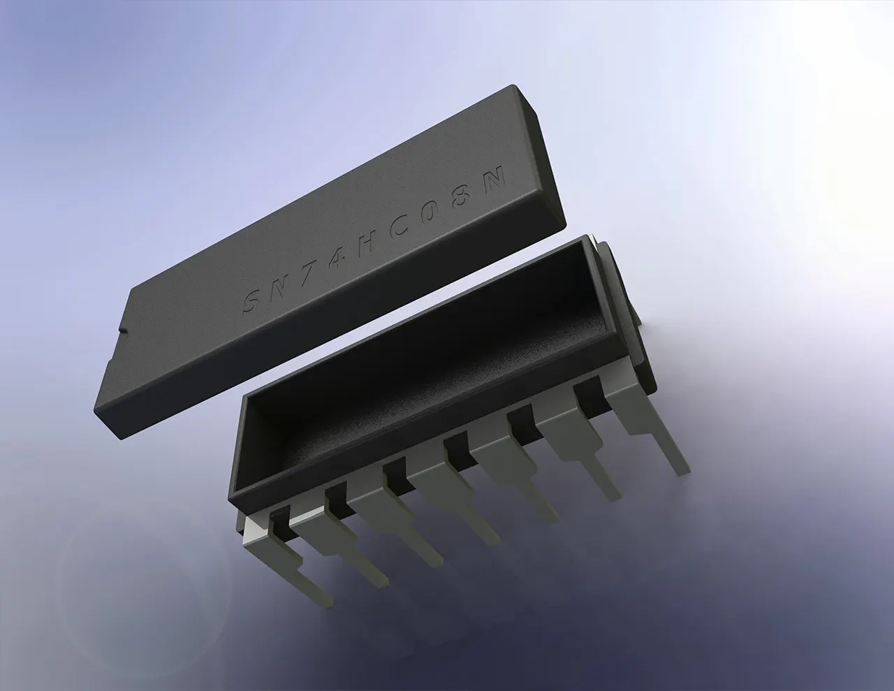
The 7408 IC is a 14-pin digital logic device that houses four independent AND gates. Each gate operates with two inputs and one output, making it a versatile component for logical operations. The pin arrangement follows a dual in-line package (DIP) configuration, which is common in integrated circuits. This layout simplifies the connection process in breadboards and printed circuit boards (PCBs).
The 7408 IC pin diagram provides a visual representation of the pin arrangement and their respective functions. It helps users identify the input, output, power supply, and ground pins. Below is a table summarizing the pin numbers and their corresponding functions:
| Pin Number | Function |
|---|---|
| 1 | A1 (Input) |
| 2 | B1 (Input) |
| 3 | Y1 (Output) |
| 4 | A2 (Input) |
| 5 | B2 (Input) |
| 6 | Y2 (Output) |
| 7 | GND (Ground) |
| 8 | VCC (Power) |
| 9 | A3 (Input) |
| 10 | B3 (Input) |
| 11 | Y3 (Output) |
| 12 | A4 (Input) |
| 13 | B4 (Input) |
| 14 | Y4 (Output) |
Note: Pins 7 and 14 are critical for powering the IC. Pin 7 connects to the ground, while pin 14 connects to the positive supply voltage.
Explanation of the 7408 IC Pinout
The 7408 IC pinout defines the specific roles of each pin in the circuit. Understanding the pinout is essential for proper integration into electronic systems. The IC features four AND gates, each with two input pins and one output pin. The inputs are labeled as A and B, while the outputs are labeled as Y. For example, Gate 1 uses pins 1 (A1) and 2 (B1) as inputs and pin 3 (Y1) as the output.
The power supply pins ensure the IC functions correctly. Pin 14 (VCC) connects to a +5V power source, while pin 7 (GND) connects to the ground. These pins provide the necessary voltage levels for the internal logic gates to operate.
The table below further explains the pinout for the 7408 IC:
| Pin Number | Function |
|---|---|
| 1 | Input A for Gate 1 |
| 2 | Input B for Gate 1 |
| 3 | Output Y for Gate 1 |
| 4 | Input A for Gate 2 |
| 5 | Input B for Gate 2 |
| 6 | Output Y for Gate 2 |
| 7 | Ground |
| 8 | Output Y for Gate 3 |
| 9 | Input A for Gate 3 |
| 10 | Input B for Gate 3 |
| 11 | Output Y for Gate 4 |
| 12 | Input A for Gate 4 |
| 13 | Input B for Gate 4 |
| 14 | VCC |
Tip: When designing circuits, always double-check the pinout to avoid incorrect connections that could damage the IC.
Pin Configuration for Standard Packages
The 7408 IC is available in various standard packages, including DIP, surface-mount device (SMD), and chip-scale packages. The pin configuration remains consistent across these formats, ensuring compatibility with different circuit designs. Below is a detailed description of the pin configuration for the DIP package, which is the most commonly used format:
| Pin | Description |
|---|---|
| Pin 1 | Input A1 - First input for the first AND gate. |
| Pin 2 | Input B1 - Second input for the first AND gate. |
| Pin 3 | Output Y1 - Output for the first AND gate. |
| Pin 4 | Input A2 - First input for the second AND gate. |
| Pin 5 | Input B2 - Second input for the second AND gate. |
| Pin 6 | Output Y2 - Output for the second AND gate. |
| Pin 7 | Ground (GND) - Connects to the ground of the power supply. |
| Pin 8 | Output Y3 - Output for the third AND gate. |
| Pin 9 | Input A3 - First input for the third AND gate. |
| Pin 10 | Input B3 - Second input for the third AND gate. |
| Pin 11 | Output Y4 - Output for the fourth AND gate. |
| Pin 12 | Input A4 - First input for the fourth AND gate. |
| Pin 13 | Input B4 - Second input for the fourth AND gate. |
| Pin 14 | Vcc - Connects to the positive supply voltage (+5V). |
This configuration ensures that the IC can be easily integrated into various applications, from educational projects to industrial systems. The consistent layout across packages simplifies the design process for engineers and hobbyists alike.
Truth Table of the 7408 IC
Logical Operation of the AND Gate
The AND gate is one of the fundamental building blocks in digital logic. It performs a logical conjunction, meaning the output is high (1) only when all inputs are high. In the case of the 7408 integrated circuit, each of its four gates operates as a quad 2-input AND gate, meaning each gate has two inputs and one output.
When both inputs of an AND gate receive a high signal, the gate produces a high output. However, if either or both inputs are low, the output remains low. This behavior makes the AND gate essential for circuits requiring conditional logic, where multiple conditions must be true for an action to occur.
Example: In a security system, an AND gate can ensure that an alarm triggers only when both a motion sensor and a door sensor detect activity simultaneously.
Truth Table for a Single AND Gate
The truth table for a single AND gate in the 7408 IC illustrates how the gate processes input signals to produce an output. The table below summarizes the input-output relationship:
| Input A | Input B | Output Y |
|---|---|---|
| L | L | L |
| L | H | L |
| H | L | L |
| H | H | H |
In this table:
-
L represents a low signal (logic 0).
-
H represents a high signal (logic 1).
This truth table demonstrates that the output is high only when both inputs are high.
Combined Truth Table for All Four Gates
The 7408 IC contains four independent quad 2-input AND gates, each functioning according to the same logical rules. The combined truth table for all four gates reflects the behavior of the IC as a whole. Each gate operates independently, processing its respective inputs to produce an output.
| Input A | Input B | Output |
|---|---|---|
| 0 | 0 | 0 |
| 0 | 1 | 0 |
| 1 | 0 | 0 |
| 1 | 1 | 1 |
The table above uses binary notation, where 0 represents a low signal and 1 represents a high signal. This format is commonly used in digital electronics to simplify representation.
To visualize the combined truth table, the chart below provides a graphical representation of the output responses for each input combination:
The chart highlights the logical behavior of the gates, emphasizing that the output is high only when both inputs are high. This consistency across all four gates makes the 7408 IC a reliable choice for implementing logical conjunctions in digital circuits.
Tip: When designing circuits with the 7408 IC, ensure that the inputs to each gate are correctly configured to achieve the desired logical operation.
The 7408 IC truth table serves as a critical reference for understanding how the IC processes input signals. By analyzing the truth table, engineers can design circuits that leverage the IC's capabilities effectively.
Detailed Pin Descriptions of the 7408 IC
Input Pins and Their Functions
The 7408 IC features eight input pins, divided into two inputs for each of its four AND gates. These pins are labeled as A and B, corresponding to the two inputs required for logical conjunction. For instance, Gate 1 uses Pin 1 (A1) and Pin 2 (B1) as its inputs. Similarly, Gates 2, 3, and 4 utilize Pins 4, 5; 9, 10; and 12, 13, respectively.
Each input pin accepts binary signals, either high (logic 1) or low (logic 0). The IC processes these signals to determine the output based on the AND gate's truth table. The input pins are compatible with CMOS, NMOS, and TTL logic families, ensuring seamless integration into various digital systems.
Tip: Always verify the input voltage levels to ensure they fall within the IC's operating range of 0V to 5.5V for optimal performance.
Output Pins and Their Functions
The 7408 IC includes four output pins, each corresponding to one of its AND gates. These pins are labeled as Y1, Y2, Y3, and Y4, located at Pins 3, 6, 8, and 11, respectively. Each output pin generates a binary signal based on the logical conjunction of its two input pins.
The table below summarizes the relationship between the input and output pins:
| Pin Number | Function |
|---|---|
| 1, 4, 9, 12 | Input A for Gates 1–4 |
| 2, 5, 10, 13 | Input B for Gates 1–4 |
| 3, 6, 8, 11 | Output Y for Gates 1–4 |
The output pins operate effectively within the IC's supply voltage range of 4.75V to 5.25V. This ensures reliable performance in diverse power environments.
Power Supply and Ground Pins
The 7408 IC requires two dedicated pins for power supply and grounding. Pin 14 (Vcc) connects to the positive supply voltage, typically +5V, while Pin 7 (GND) connects to the ground. These pins provide the necessary electrical power for the IC's internal logic gates to function.
Proper connection of these pins is crucial for the IC's operation. The power supply pin ensures stable voltage levels, while the ground pin completes the circuit. Incorrect wiring of these pins can lead to malfunction or damage to the IC.
Note: To prevent voltage fluctuations, use decoupling capacitors near the power supply pin in your circuit design.
The 7408 IC's pinout simplifies its integration into digital systems, making it a versatile choice for logic-based applications.
Specifications and Ratings of the 7408 IC
Maximum Ratings
The 7408 IC is designed to operate within specific limits to ensure reliability and performance. Exceeding these limits can damage the IC or cause malfunction. The table below summarizes the maximum ratings for the ic 7408:
| Specification | Value |
|---|---|
| Supply Voltage | Up to 7V |
| Input Voltage | Up to 5.5V |
| Operating Temperature | -55°C to 125°C |
| Storage Temperature | -65°C to 150°C |
The IC's robust temperature range makes it suitable for both industrial and educational applications. However, users must ensure that the supply voltage and input voltage do not exceed the specified limits.
Operating Conditions
For optimal performance, the 7408 IC must operate within its recommended conditions. The table below outlines the key parameters:
| Parameter | Value |
|---|---|
| Voltage Rating | 2.0 to 6.0V |
| Temperature Rating | 0°C to 70°C |
These conditions ensure the IC functions reliably in standard environments. The voltage range supports compatibility with various power supplies, while the temperature range suits most consumer and educational projects.
Tip: Always verify the power supply and ambient temperature to maintain the IC's longevity.
Electrical Characteristics
The electrical characteristics of the ic 7408 define its behavior under normal operating conditions. These specifications help engineers design circuits that utilize the IC effectively. The table below highlights key characteristics:
| Characteristic | Specification |
|---|---|
| Input High Voltage (VIH) | At least 2V |
| Input Low Voltage (VIL) | No more than 0.8V |
| Output High Voltage (VOH) | At least 2.4V at 4mA |
| Output Low Voltage (VOL) | No more than 0.4V at 8mA |
| Power Dissipation | Up to 10mW per gate |
The IC operates efficiently with minimal power dissipation, making it ideal for low-power applications. Its input and output voltage levels ensure compatibility with other digital components.
Note: Proper grounding of the IC's GND pin is essential to achieve accurate electrical performance.
The specifications and ratings of the 7408 IC provide a comprehensive understanding of its capabilities. By adhering to these parameters, users can ensure reliable operation in a wide range of digital circuits.
Switching Characteristics
The switching characteristics of the 7408 IC define how quickly its internal logic gates respond to changes in input signals. These parameters are crucial for designing circuits that require precise timing and high-speed operation.
Propagation Delay
Propagation delay refers to the time taken by the IC to process an input signal and produce the corresponding output. For the 7408 IC, this delay typically ranges between 10 nanoseconds (ns) and 20 nanoseconds (ns), depending on the operating conditions.
Note: Lower propagation delay ensures faster response times, making the IC suitable for high-speed digital systems.
Rise and Fall Times
Rise time measures how long it takes for the output signal to transition from a low state (0) to a high state (1). Fall time, on the other hand, indicates the duration of the transition from high to low. The 7408 IC exhibits rise and fall times in the range of 15 ns to 25 ns, ensuring smooth signal transitions.
Switching Frequency
The IC supports a maximum switching frequency of several megahertz (MHz). This frequency determines how quickly the IC can toggle between states without compromising performance.
| Parameter | Typical Value |
|---|---|
| Propagation Delay | 10–20 ns |
| Rise Time | 15–25 ns |
| Fall Time | 15–25 ns |
| Maximum Switching Frequency | Several MHz |
Factors Affecting Switching Characteristics
Several factors influence the switching characteristics of the 7408 IC:
-
Supply Voltage: Higher voltage levels reduce propagation delay.
-
Temperature: Extreme temperatures can increase delay times.
-
Load Capacitance: Larger capacitance slows down signal transitions.
Tip: To optimize switching performance, maintain stable voltage levels and minimize load capacitance in circuit designs.
The 7408 IC's switching characteristics make it a reliable choice for applications requiring precise timing and rapid signal processing. Understanding these parameters helps engineers design efficient and responsive digital systems.
Applications of the 7408 IC
Use in Basic Logic Circuits
The 7408 integrated circuit is a fundamental component in basic logic circuits. Its four independent AND gates allow it to perform logical conjunctions efficiently. Engineers often use it to design circuits that require conditional operations. For example, a simple circuit using the 7408 can ensure that a light turns on only when two switches are activated simultaneously. This makes it ideal for projects requiring precise logical decisions.
The IC's straightforward pin configuration simplifies its integration into breadboards and printed circuit boards. Each AND gate operates independently, enabling the creation of multiple logic functions within a single circuit. Its compatibility with standard voltage levels ensures seamless operation in educational and professional projects.
Applications in Microcontroller-Based Systems
The 7408 integrated circuit plays a vital role in microcontroller-based systems. It enhances the logical capabilities of microcontrollers by performing external AND operations. This is particularly useful in systems where multiple conditions must be met before triggering an action. For instance, a microcontroller can use the 7408 to process sensor inputs, ensuring that an output is activated only when all required conditions are satisfied.
Practical experiments highlight the IC's importance in such systems. One project demonstrates how to create an AND gate circuit using the 7408, showcasing its functionality in digital logic. The hands-on approach helps users understand its operation within a microcontroller context. This versatility makes the IC a valuable tool in robotics, automation, and embedded systems.
Role in Signal Processing and Control Systems
The 7408 integrated circuit is widely used in signal processing and control systems. Its ability to combine multiple input signals into a single output makes it essential for filtering and decision-making processes. For example, in industrial automation, the IC can ensure that a machine operates only when all safety conditions are met.
The IC's fast switching characteristics and low power consumption make it suitable for high-speed signal processing. Its robust design allows it to function reliably in harsh environments, making it a preferred choice for control systems in automotive and aerospace applications. The 7408's consistent performance ensures accurate and efficient operation in critical systems.
The 7408 IC stands out as a fundamental component in digital electronics. Its pin diagram and pinout simplify integration into circuits, while the truth table highlights its logical AND operation. Engineers and students alike benefit from its versatility in applications such as signal processing, microcontroller systems, and basic logic circuits.
Key Takeaway: The 7408 IC combines reliability, efficiency, and ease of use, making it indispensable for both educational and professional projects. Its role in enabling logical operations ensures its continued relevance in modern digital systems.
FAQ
What is the primary function of the 7408 IC?
The 7408 IC contains four independent AND gates. Each gate performs a logical conjunction, producing a high output only when both inputs are high. This makes it essential for implementing conditional logic in digital circuits.
Can the 7408 IC work with other logic families?
Yes, the 7408 IC is compatible with CMOS, NMOS, and TTL logic families. Its input and output voltage levels align with these standards, ensuring seamless integration into diverse digital systems.
How do you power the 7408 IC?
Connect Pin 14 to a +5V power supply and Pin 7 to ground. These pins provide the necessary voltage for the IC to operate. Proper wiring ensures stable performance and prevents damage.
What happens if one input of an AND gate is low?
If one input is low, the AND gate's output will always be low, regardless of the other input's state. This behavior follows the logical conjunction rule of the AND gate.
Is the 7408 IC suitable for high-speed applications?
Yes, the 7408 IC supports fast switching with a propagation delay of 10–20 nanoseconds. Its high-speed performance makes it ideal for applications requiring quick response times.
Tip: Always check the IC's voltage and temperature ratings to ensure reliable operation in your circuit designs.
Written by Jack from AIChipLink.
AIChipLink, one of the fastest-growing global independent electronic components distributors in the world, offers millions of products from thousands of manufacturers, and many of our in-stock parts is available to ship same day.
We mainly source and distribute integrated circuit (IC) products of brands such as Broadcom, Microchip, Texas Instruments, Infineon, NXP, Analog Devices, Qualcomm, Intel, etc., which are widely used in communication & network, telecom, industrial control, new energy and automotive electronics.
Empowered by AI, Linked to the Future. Get started on AIChipLink.com and submit your RFQ online today!


.png&w=256&q=75)


